Electronics inspection: Infrared imaging microscopes aid in detecting integrated circuit defects
Radiant Optronics (Singapore, Singapore;www.radiantoptronics.com) has developed an infrared (IR) microscope that is used to inspect integrated circuits (IC) for internal defects or cracks that may occur during the manufacturingprocess.
Wafer is a thin substrate of semiconductor material that is used in electronics for IC fabrication. There are many types of semiconductor materials and one of the most commonly materials used in electronics is Silicon (Si).
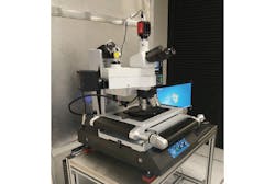
Radiant Optronics has developed an IR microscope fitted with a SWIR camera that inspects ICs for internal defects or cracks.
Silicon wafer, a key component in ICs, is formed from highly pure, nearly defect-free, monocrystalline silicon sliced from a silicon boule. Serving as the substrate for microelectronic devices that are built in and over the thinly sliced silicon wafer, the wafer ultimately undergoes a multitude of microfabrication process steps such as masking, etching, doping, andmetallization.
ICs, which have become the main component of nearly all electronic devices, are comprised of a microscopic array of electronic circuits and components that has been implanted onto the surface of a single crystal of semiconductor material such as silicon. Within the integrated circuit, components, circuits, and base materials are all made together out of a single piece of silicon wafer. Hundreds of integrated circuits are made at the same time on a single, thin slice of silicon wafer and then they are cut apart into individualIC chips.
Wafers accumulate residual stress during the growth, sawing, grinding, etching and polishing process, and cracks may be generated throughout all of these processes. Cracks may also occur when the integrated circuits themselves are cut into individual ICs. If undetected, wafers can be rendered unusable in subsequent manufacturing stages. As a result, it is important to inspect the raw material substrate for impurities before processing and detect any defects during processing, in order to reduce waste and keepcostdown.
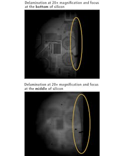
InGaAs cameras operating in the SWIR wavelength band from 0.9 μm to 1.7 μm acquire images that highlight defects within the silicon wafer.
By using indium gallium arsenide (InGaAs) cameras operating in the short-wave infrared (SWIR) wavelength band from 0.9 μm to 1.7 μm, it is possible to see through semiconductor silicon substrates. This ability to see through the material enables manufacturers to generate infrared images that will highlight defects such as cracks within the siliconwafer.
Radiant Optronics—a company that has a strong focus in the semiconductor field, wafer fabrication, service laboratories, packaging, and PCB assembly in Asia—has developed an infrared imaging microscope that IC manufacturers can use to inspect for internal defects and cracks.
The microscope utilizes a Goldeye G-008 SWIR camera from Allied Vision (Stadtroda, Germany; www.alliedvision.com), which features a 320 x 256 InGaAs sensor with a 30 μm pixel size and is sensitive in the short-wave infrared spectrum from 0.9 μm to 1.7 μm at up to 344 fps. The SWIR camera—which is thermo-electrically cooled for low-noise images—has a GigE Vision interface, a compact form factor (55 mm x 55 mm x 78 mm), as well as Allied Vision’s Vimba software development kit, which enables users and developers to program their own applications across Windows and Linux platforms.
“The Goldeye G-008 is a low-resolution model with an affordable price. The low resolution is sufficient to detect the defects, so it is the ideal choice for this cost-sensitive application. Our customers can benefit from the Goldeye’s outstanding performance and we enjoy support from Allied Vision’s Asia-Pacific office just next door in Singapore,” explained Christopher Cheong, Director of Radiant Optronics.


