Optical/imaging system and nondestructive testing find coated-wire flaws
Optical/imaging system and nondestructive testing find coated-wire flaws
By Åse M. Ballangrud and Norman N. Axelrod
An optical, noncontact, sensing and imaging test system is providing continuous product, process, and quality control of an extrusion process that applies a clear plastic coating on small-diameter wire used to form the electrical leads for implantable medical devices. Before implementing this on-line system, the wire manufacturer was detecting defects in the plastic coating--after the process was completed--in only the first and last 100 feet of a spool of wire that would range in length from 10,000 to 80,000 ft. Now, by implementing an optical/imaging nondestructive test system, the manufacturer obtains fully documented noncontact inspections of the entire spool of wire.
The test system also proves effective in process control because it delivers real-time data results. The data are used to adjust the extrusion process and therefore prevent the production of long lengths of unusable, out-of-tolerance coated wire, which often happened before the new test system was installed.
Two signal-processing techniques--SmartOptics and RobustSystems--form the core of the computer-based nondestructive test system. The SmartOptics technique modifies the test light signals before they reach a digital camera or photodetector and, therefore, before detailed digital-signal processing and rejection decisions are made. This approach eliminates all the background images and produces signals only from the images` critical features of interest. In this manner, the technique increases both the imaging contrast and the signal-to-noise ratio (S/N).
The use of optical hardware to boost the system`s S/N increases system speed and reliability over the use of software for signal enhancement. Moreover, by minimizing noise, the test system eliminates the phantom or ghost signals that can emerge with feature extraction from noisy images.
The RobustSystems methodology provides software tools for systematically exploiting all knowledge about a target to make the total sensing system more robust. The methodology provides means to automatically compensate for acceptable background variations by hardware and software design; adapt for changes in the product and the system that are not related to the target(s) of interest by real-time recalibration during operation; verify that the results are physically plausible and that constraints are not exceeded; and evaluate the measurement to assure quality of test data.
Exploiting optics
By modifying the light before it strikes a photodetector or camera, the SmartOptics optical-design elements exploit the optical variations related to changes in test materials, structures, and processes to enhance the system S/N or optical contrast. As many as four classes of properties can be used to discriminate a feature of interest from background noise--geometry, spectral properties, polarization properties, and induced optical characteristics. Appropriate optics are matched to specific properties of the material under test.
In detecting wire-coating defects, a high-resolution optical defect-detection assembly is positioned to ensure that mirror-like reflections are not detected. For proper gauging tests, the sensing assembly optically detects the wire interfaces to avoid the coating appearing to be vanishingly small when examination by a microscope shows otherwise.
Real-time signal information enables automatic corrective actions when defects in the wire coating occur. Timely knowledge of coating-wire defects, thickness, ovality, and eccentricity is critical to maintaining close tolerances. Further, noncontact sensing of coating-thickness variations and defects can be obtained throughout an entire coating run without defect-inducing handling.
The nondestructive coated-wire test system uses nine sensors and three computers. It can measure coating thickness to ۪.01 mil (0.00001 in.), detect 1-mil defects, and provide process-control signals, real-time displays, and production and statistical summaries. The test system was developed, installed, and validated using US Food and Drug Administration general manufacturing procedures.
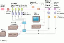
During the initial medical-device manufacturing step, the wire is fed through an extruder that applies the plastic coating. After a cooling-bath operation, the coated wire is directed through Station 1 (see Fig. 1). The entire system comprises four inspection stations spaced over a span of 30 to 40 feet, all under computer control. Station 1 performs as a capacitive-type pinhole-defect detector. The next station is a light-based outside-diameter-variation detector that serves as a process-control station; it sends feedback signals to the extruder to correct any drift in coating thickness. Station 3 uses digital-vision gauging techniques with two video cameras and a video monitor. The last station uses four sets of optics and photosensors to perform optical defect detection.
A footage counter and a defect marker can be installed as an optional fifth station. The marker places a crimp mark at the location of any defects; these defects are so small that they can be seen only under a microscope. The defects are subsequently trimmed from the coated wire. The footage counter keeps track of the length of the wire spool and of the defect positions.
System details
At Station 1, initial pinhole detection is accomplished using a capacitive-type measuring instrument from Beta Instrument Co. Ltd. (High Wycombe, England). It was already being used by the medical-device manufacturer before systems integrator Norman N. Axelrod Associates (New York, NY) was approached to develop a complete nondestructive test system.
A KW20 diameter-variation detector from Zumbach Electronics Corp. (Mt. Kisco, NY) is used at Station 2 as a separate optical system. It continuously monitors the coated wire`s outside diameter in two perpendicular directions. Irregularities such as knots and neckdowns that are created during the extrusion process are therefore uncovered. The detector measures variations in the outer diameter of the coated wire as it passes through a zone of parallel light, which is focused onto a photocell at the receiving end of the beam. The parallel light projected at the wire allows the discrimination of true irregularities from radial wire movements.
At Station 3, coating-thickness measurements are performed by two computer-controlled digital-vision-gauging video cameras from Panasonic Medical & Industrial Video Co. (Secaucus, NJ). These cameras are linked to a frame-grabber board from Imaging Technology Inc. (Bedford, MA), which is housed in a personal computer from Compaq Computer Corp. (Houston, TX).
Optical defect-detection Station 4 consists of four computer-controlled, fiberoptic-cabled channels that identify defects in four 90 zones around the wire. The tungsten halogen light source and fiberoptics are supplied by Dolan-Jenner Industries (Lawrence, MA). The detectors are photodiodes from Hamamatsu Corp. (Bridgewater, NJ) that are coupled to custom-developed operational amplifier circuits in a custom housing manufactured by Axelrod Associates. The sensor electronics reside on an analog-to-digital converter board from Keithley-Metrabyte (Cleveland, OH), which is housed in another Compaq computer.
A third Compaq computer acts as the overall control console. It accepts signals from all the system sensors using an A/D converter, RS-232 communication, 4 to 20 mA, and TTL signals to control all system responses and to record, analyze, and display all the data.
Gauging measurements
Compensation techniques, consistency of the dimensions of several components, and data consistency are all used to assure system-gauging results. For example, 14 scan lines are analyzed in each captured image of monofilament wire from the two video cameras that monitor coating thickness. During image processing, the values for the two thickest and the two thinnest coatings are eliminated. Then, the remaining 10 lines are averaged and used to determine the coating thickness. This approach provides measured values to ۪.01 mil (0.00001 in.), with a 99% confidence limit, as determined by the system user.
Wire thickness is measured and controlled to be within a given range. If the coating is either too thick or too thin, the location of this unacceptable condition is recorded and a visible mark is made on the moving coated wire. A signal is also delivered to the extruder, which immediately adjusts the thickness to an acceptable value.
The thickness measurement itself is also assessed to assure consistent results. The spread of the measured thicknesses is determined by calculating the root-mean-square (rms) value from the 10 values obtained from the imaging scan lines. This spread value provides a quality factor for the thickness measurement. If the rms value is large, an unacceptably large variation in the 10 thickness values exists. This indicates that either the material or the measurement is unacceptable and requires attention.
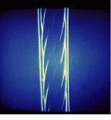
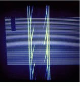
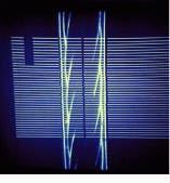
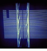
The nondestructive test procedure for coated, braided, multistrand-twisted wire is extended by increasing the number of scan lines to 50 to determine the minimum coating thickness (see Fig. 2). The coating thicknesses are sorted, and the smallest values are used to determine the minimum coating thickness. The two smallest values are discarded to reduce the possibility of detecting local imperfections, because the objective in this assessment is gauging, not defect detection. The dark line down the middle of the photo in Fig. 2 represents the average position from the outer coating on the left and right wires.
Adaptation and compensation
In this nondestructive test system, compensation is used in optical defect detection to reduce the effects of changing conditions. All the defect-detection sensing channels use illumination from the same tungsten halogen light source. Signals from adjacent channels are compared digitally. Any variation between adjacent channels is detected as a defect.
The system adapts to possible changes in channel-to-channel performance. Each channel used for optical defect detection is recalibrated repeatedly during production by averaging 200 defect-sensing measurements. The updated values are used to upgrade the comparison of adjacent channels, thereby adapting the system to possible changes in channel-to-channel sensor performance.
The system uses both compensated hardware and software designs and provides dynamic real-time calibration by using the RobustSystems methodology. This approach compensates and adapts for variations in light-source intensity and for slow variations in material properties.
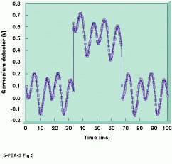
To determine the effectiveness of compensation for light-source intensity variations, individual points are plotted on a graph (see Fig. 3). These points are the sensor signals acquired by the station computer using an analog-to-digital converter operating at a data-acquisition rate of 4000/s. Adjacent data points were acquired 0.25 ms apart.
Note that the detector signal jumps in voltage value at the 34-ms point. This jump occurs because the detector is responding to a light-emitting diode source that is being rapidly turned on and off to demonstrate that the photosensor amplifier response time is less than 0.25 ms. When adjacent sensors are accessed 0.25 ms apart, the adjacent sensors see substantially the same light intensity unless a defect exists.
Differences in signals from adjacent points are more than 10 times less than the amplitude changes in the signals over tens of milliseconds. This property permits the use of ac-powered incandescent lamps (which have about 10% to 15% modulation from the 60-cycle ac) with an effective difference in intensity at the two sensors of 1% to 2%. The source used in Fig. 3 was a fluorescent lamp.
Operator involvement
The nondestructive test system provides visual aids to keep operators informed and involved. For gauging, the locations of wire edges found by the computer are registered on a video monitor by black rectangles at the appropriate positions on the scan lines; vertical lines on the dark background represent the left and right coatings. When the displayed monitor image represents a 2-mil coating on a 5-mil wire, the asymmetry in the coating can be seen on the monitor from a long distance. This visual aid, plus computer-monitor displays of coating thicknesses (at different angles around the wire), has reduced the system set-up time prior to extrusion from 24 hours to between two and six hours.
Åse M. Ballangrud is an associate and Norman N. Axelrod is the principal in the consulting firm of Norman N. Axelrod Associates, New York, NY 10036.
FIGURE 1. In the optical-sensing, digital-imaging, nondestructive testing system, coated wire moves from right to left through five test stations: pin-hole detection, outside diameter variation, digital vision gauging, optical defect detection, and an optional footage counter and defect marker.
FIGURE 2. The two vertical straight lines in the image (top) represent the outer surfaces of plastic-coated multistrand twisted wire. The curved lines are the edges of the coating on the nearest wire. In other images (second and third), 50 scan lines are used for coating detection. The small rectangular space that extends through the top 10 lines, at the upper left of these images, marks the area where the light-source intensity was monitored. In another image (bottom), the curved black lines show the locations where the computer determined the edges to be.
FIGURE 3. This graph shows the detector output voltage over time and represents the effectiveness of compensation for light-source intensity. The individual points appearing as rectangles are sensor signals acquired by a computer using an A/D converter operating at a rate of 4000 samples/s. The detector signal jump at approximately 34 ms occurs in response to the detector receiving light from an LED that is rapidly cycling on and off.
