CCD/CMOS sensors spot niche applications
By targeting specific applications and select market segments, sensor vendors are avoiding head-on competition and ensuring market share and revenues.
By Andrew Wilson, Editor
Although they have dominated the imaging market for decades, CCD sensors are now being threatened by low-cost unipolar CMOS-based devices. Although CCD imagers produce high-quality images, they are expensive, consume relatively large amounts of power, and require supporting circuitry. On the other hand, CMOS sensors use "standard CMOS processes," require little or no supporting circuitry, and offer low-cost, fully integrated system-on-a-chip platforms.
Clever marketing campaigns presented over the past few years extolled the virtues of CMOS sensors, but those devices have fallen short on implementation. Whereas system-on-a-chip platforms can be accomplished with CMOS imagers, there is no standard unipolar process to manufacture them—each process must be especially tailored for each sensor. And, while CMOS imagers can cost less than their CCD counterparts, their image quality does not equal that of CCDs. However, in mass markets such as those for mobile telephones, PDAs, security cameras, optical mice, and toys, high volume and low cost—not image quality—are the most important marketing parameters.
Accordingly, companies such as Pixim (Mountain View, CA, USA), Fujitsu Microelectronics America (Sunnyvale, CA, USA), and PixArt (Hsin-Chu, Taiwan) are competing for a relatively large, high-volume, low-cost sector. If the CMOS marketing hype is correct, then such devices should be able to be used as CCD replacements. But, according to Emi Igarashi, director of marketing communications at Fujitsu
Microelectronics America, the company has no designed-in products in medical, military, scientific, or machine-vision applications. "Our current emphasis is high-volume applications such as cell phones, PDAs, and hand-held PCs," he says.
Pixim is using the same tactic. "We are not targeting scientific markets now," says Robert Siegel, executive vice president. "Our primary market is security cameras. Although we have spoken with firms in other markets, we do not have design wins yet."
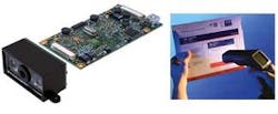
Symagery (Kanata, ON, Canada) also offers its CMOS imagers and development kits to OEMs building portable hand-held products. As well as offering the VCA1281C, a 1280 × 1024-pixel CMOS imaging array, on-board programmable gain amplifier, and 8-bit ADC, the company provides its ImageLift image reader based on the sensor (see Fig. 1). As an imaging module targeted at applications such as optical character recognition and one- and two-dimensional barcode reading, the reader has recently been incorporated into the Anywhere Imager image scanner from Siemens Dematic (Arlington, TX, USA).
According to Mike Keenan, vice president, marketing, at Symagery, Siemens is using the USB2 port from ImageLift to transfer images to a host CPU in the Anywhere Imager. The system captures handwritten address blocks, 1-D/2-D barcodes, and other pertinent mailing information. For hard-to-read address blocks and other information, the system decodes the information and then relabels the mail pieces for the remainder of the automation process. "This function, called exception scanning, further automates the mail-handling process," says Keenan.
Low light levels
Rather than develop standard CMOS imagers, companies such as Silicon Vision (Boxdorf, Germany), FillFactory (Mechelen, Belgium), and SMaL Camera Technologies (Cambridge, MA, USA) are tailoring their CMOS designs for special applications. Notably, these applications include low-light-level and high-speed imaging.
In the design of its LARS III image sensor, Silicon Vision combines both amorphous silicon and crystalline silicon materials in a single circuit that results in a vertically integrated hybrid (thin film on ASIC) TFA/CMOS sensor (see Vision Systems Design, January 2003, p. 7). This locally auto-adaptive sensor splits pixel data into two separate signals, both with dynamic-range requirements below 70 dB. As each pixel controls its integration duration automatically within the defined integration time set for the whole imager, integrated capacity and individual time-stamp data are captured as analog values in each pixel and read at the end of the full integration time. Both signals are then recombined on-chip to produce a linear dynamic-range image of 120 dB.
To achieve a similar dynamic range, FillFactory uses a logarithmic photo transfer in the design of its Fuga series of image sensors. By log-compression of the input optical power scale onto a linear-output voltage scale, the device can achieve a logarithmic response of greater than 120 dB. Therefore, the Fuga series can be used to view scenes with vastly different luminances in the same image without the need for setting an exposure time.
Using a similar technique, the IM-001 series of VGA CMOS image sensors from SMaL Camera Technologies can also achieve a 120-dB dynamic range. Using the company's proprietary Autobrite technology, the IM-001 can be supplied as a single device or as part of an OEM development board. Currently, the company is targeting the consumer and embedded automotive market with its products. When used in automotive applications, conventional cameras are unable to adapt to varying lighting conditions. Using the company's Autobrite technology, however, results in images in which the features are more discernable (see Fig. 2).
High-speed designs
In addition to featuring logarithmic response, CMOS imagers can be randomly addressed, a feature that makes them useful in high-speed imaging applications. To meet such demands, sensor vendors are tailoring their CMOS and CCD designs. Whereas FillFactory's 1.3-Mpixel, 450-frame/s LUPA1300 image sensor is offered as a standard product, custom versions of the device have been developed for Redlake MASD (San Diego, CA, USA), Vision Research (Wayne, NJ, USA), and SciMedia (Irvine, CA, USA).
Developed jointly by the Institute of Physical and Chemical Research (RIKEN BSI; Saitama, Japan) and the Stanley Electric Company (Tokyo, Japan) for high-speed image-capture applications, SciMedia's MiCAMultima uses a 100 × 100-pixel image sensor from FillFactory to capture up to 4 s of images at 10,000 frames/s. With a dynamic range of approximately 96 dB, the camera features a quantum efficiency of 50% across the 600- to 800-nm spectrum. For applications that do not require such high speeds, FillFactory's devices also can be found in the Redlake HG-100K 1504 × 1128-pixel camera capable of 1000 frames/s and Vision Research's Phantom V7.0 4800-frame camera with an 800 × 600-pixel imager (see Fig. 3).
But the CMOS device vendors are not the only ones focused on the high-speed imaging market. The department of electrical engineering and computer science at the University of Osnabrück (Osnabrück, Germany) has recently developed a high-speed video camera called Hyper Vision that is capable of capturing 1 million frames/s. Developed jointly with Kinki University (Osaka, Japan), Shimadzu Corp. (Kyoto, Japan), and Philips/Dalsa (Waterloo, ON, Canada), the camera is based on a CCD architecture called an in situ storage image sensor. In its design, each of the 312 × 260 pixels of the sensor has its own on-chip memory that can capture 100 continuous images at full-frame rate. According to professor Arno Ruckelshausen of the University of Osnabrück, the camera will be commercially available through Shimadzu.
Architectures and applications
With some sensor vendors targeting low-light-level and high-speed applications, others are building sensors for semiconductor, security, and medical applications. These image sensors are using novel and often proprietary fabrication techniques to achieve the required sensitivity at specific imaging wavelengths, such as ultraviolet (UV) and x-ray.
According to Robin Dawson, head of solid-state imaging at Sarnoff Corp. (Princeton, NJ, USA), accurately characterizing nanoscale features is critical to the deep-submicron semiconductor industry, and visible light imaging is no longer adequate. "Although UV imaging can be used," he says, "the results have to be both uniform and consistent." To meet these demands, Sarnoff Corp. has developed a 1024 × 1024 × 14-bit back-illuminated CCD UV camera module with a 100% fill factor and a greater-than 55% quantum efficiency for the 200- to 800-nm range. According to Dawson, a semiconductor-equipment manufacturer is using this UV VIS1M100 camera to measure feature sizes that are virtually impossible to visualize with visible light.
In applications ranging from medical and scientific imaging to industrial inspection and security, x-ray imaging is often used. To capture frequencies at these wavelengths, designers can choose from a number of different imager designs that include CMOS imagers and CCDs.
In the development of its C7942 large-area, single-crystal, x-ray CMOS image sensor, for example, Hamamatsu (Bridgewater, NJ, USA) has developed a 2400 × 2400 × 12-bit imager with a 30-frame/s rate and a 90% fill factor. To capture x-rays, the 120 × 120-mm CMOS wafer is coupled to the company's proprietary CsI scintillator, which converts the x-rays into photons that can be detected by the CMOS sensor. Designed with a digital video output, the C7942 sensor can be directly connected to commercially available frame grabbers.
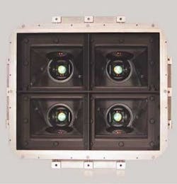
Rather than choose such CMOS imagers for the design of its digital optical detector (dOd), however, engineers at Swissray (Elizabeth, NJ, USA) have opted for CCD-based devices from Kodak Image Sensor Solutions (Rochester, NY, USA). The dOd uses optics from LINOS Photonics Inc. (Milford, MA, USA) to focus four CCD cameras on a CsI scintillator screen. Each full-frame CCD captures the image of one quadrant with a 10% overlap on adjacent quadrants. The final image is then stitched together from these four images to produce a seamless result (see Fig. 4).
By targeting applications in specific scientific, medical, industrial, and military applications, sensor vendors can avoid competing in low-cost, high-volume markets. Whereas PDAs, digital cameras, computers, cell phones, and other consumer products will account for the highest volume of imagers shipped, the cost per unit will be very low. By concentrating on more niche applications, however, sensor vendors such as FillFactory, Dalsa, and Kodak are expected to achieve profits by producing more-expensive and targeted products at lower volumes...
Company Info
Dalsa www.dalsa.com
FillFactory www.fillfactory.com
Fujitsu Microelectronics America www.fma.fujitsu.com
Hamamatsu Photonics usa.hamamatsu.com
Kinki University www.city.iizuka.fukuoka.jp/english/culture/kindai.html
Kodak Image Sensors www.kodak.com/global/en/digital/ccd/sensorsMain.jhtml
LINOS Photonics Inc. www.linos-photonics.com
Philips Semiconductors www.semiconductors.philips.com
PixArt www.pixart.com.tw
Pixim www.pixim.com
Redlake MASD www.redlake.com
RIKEN BSI www.riken.go.jp
Sarnoff Corp. www.sarnoff.com
SciMedia www.scimedia.com
Shimadzu Corp www.shimadzu.com
Siemens Dematic Postal Automation www.pa.siemens-demantic.com
Silicon Vision AG www.siliconvision.de
SMaL Camera Technologies www.smalcamera.com
Stanley Electric Co www.stanley.co.jp
Swissray International www.swissray.com
Symagery Microsystems www.symagery.com
University of Osnabr¸ck www.uni-osnabrueck.de/en/
Vision Research www.visiblesolutions.com


